
© 2007-2017 Microchip Technology Inc. DS30009715D-page 1
PIC24F Flash Program Memory
HIGHLIGHTS
This section of the manual contains the following major topics:
1.0 Introduction ....................................................................................................................... 2
2.0 Program Memory Architecture.......................................................................................... 2
3.0 Table Operation Instructions ............................................................................................. 8
4.0 Flash Memory Programming........................................................................................... 13
5.0 Program Space Visibility and Extended Data Space (PSV and EDS)............................. 21
6.0 Error Correcting Code (ECC).......................................................................................... 21
7.0 Low-Power Operation ..................................................................................................... 21
8.0 Register Map................................................................................................................... 22
9.0 Related Application Notes............................................................................................... 23
10.0 Revision History.............................................................................................................. 24

dsPIC33/PIC24 Family Reference Manual
DS30009715D-page 2 © 2007-2017 Microchip Technology Inc.
1.0 INTRODUCTION
All PIC24F devices have an internal programmable Flash array for the execution of user code.
The high-endurance Flash array provides great flexibility in code development and storage,
combining a long retention life with a high number of read/write cycles.
2.0 PROGRAM MEMORY ARCHITECTURE
PIC24F devices address a 4M x 24-bit program memory address space, as shown in Figure 2-1.
The program memory map is equally divided into the user memory space (000000h to 7FFFFFh)
and the configuration (or test) memory space (800000h to FFFFFFh).
The user program space contains the Reset vector, Interrupt Vector Tables (IVTs) and program
memory. There are three methods for accessing program space:
1. The 23-bit Program Counter (PC).
2. Table Read (TBLRD) and Table Write (TBLWT) instructions.
3. By mapping any 32-Kbyte segment of program memory into the data memory
address space.
Implemented program memory can be further divided into the vector area, which includes the
Reset and interrupt vectors, and the code area, which also includes the Flash configuration data.
Accessing unimplemented areas of the user program space (i.e., above the upper implemented
boundary of program memory) will cause an illegal address trap.
Note: This family reference manual section is meant to serve as a complement to device
data sheets. Depending on the device variant, this manual section may not apply to
all PIC24F devices.
Please consult the note at the beginning of the “Flash Program Memory” chapter
in the current device data sheet to check whether this document supports the
device you are using.
Device data sheets and family reference manual sections are available for
download from the Microchip Worldwide Web site at: http://www.microchip.com

© 2007-2017 Microchip Technology Inc. DS30009715D-page 3
PIC24F Flash Program Memory
Figure 2-1: Default Program Space Memory Map for PIC24F Devices
000000h
FEFFFEh
FFFFFFh
00xx00h
(1)
00xxFEh
(1)
Configuration Memory Space
User Memory Space
Legend: Memory areas are not shown to scale.
Note 1: The vector area extends to 0000FEh in devices with original IVT mapping. See text and Figure 2-2 for the lower
boundary of the vector area in devices with newer IVT mapping.
2: Exact boundary addresses are determined by the size of the implemented program memory and number of
Configuration registers.
3: Devices with J-Flash program memory only. See Section 2.3 “Flash Configuration Data (PIC24FJ Devices
Only)” for more information.
4: Not all devices have memory-mapped write latches. Refer to the specific device data sheet for details, including
number of latches implemented and upper address boundary.
DEVID (2)
Reserved
FF0000h
800000h
7FFFFEh
Reserved
xxxx00h
(2)
xxxxFEh
(2)
Unimplemented
Read ‘
0
’
FF0002h
FF0004h
F7FFFEh
F80000h
F800xxh
(2)
F800xxh
(2)
Device Configuration Registers
F9FFFEh
FA0000h
FA00xxh
FA00xxh
Flash Write Latches (Mapped)
(4)
Vector Area
User Flash Program Memory
Flash Configuration Words
(3)

dsPIC33/PIC24 Family Reference Manual
DS30009715D-page 4 © 2007-2017 Microchip Technology Inc.
2.1 Vector Area
The vector area starts at the beginning of program memory space, at 000000h. It contains the
master Reset vector, the hardware trap vectors and the Interrupt Vector Tables (IVTs) for all
implemented hardware interrupts. Hardware trap vectors immediately follow the Master Reset
address. The hardware interrupt vectors immediately follow the trap vectors, always starting with
Interrupt Vector 0.
The exact implementation of the vector area falls into one of two categories. Most PIC24F
devices use the original, fixed IVT mapping. Some newer PIC24F devices, particularly those that
implement CodeGuard™ security, use a different mapping. Refer to the device-specific data
sheet to determine which version is implemented. Figure 2-2 shows the structure of the different
mappings.
2.1.1 ORIGINAL IVT MAPPING
In the original PIC24F families and many subsequent PIC24F device families, the vector area is
a fixed region that extends to 0001FEh. The IVTs provide space for 8 hard trap vectors and
118 interrupt vectors.
For the main IVT, trap vectors extend from 000006h to 000012h. Interrupt vectors extend from
Vector 0 at 0000014h, to Vector 117 at 0000FEh.
The Alternate IVT (AIVT) duplicates the structure of the IVT and can be used to store addresses
for alternate exception handling. The AIVT directly follows the IVT, with trap vectors from
000106h to 000112h and interrupt vectors from 000114h to 0001FEh.
Both IVT and AIVT are implemented and available on all devices.
2.1.2 NEWER IVT MAPPING
Newer PIC24F devices implement essentially the same IVTs as in the original mapping (although
some of the hard trap vectors may reside at different addresses within the same address range).
Unlike devices with original IVT mapping, the AIVT is not permanently allocated in program
memory at a fixed address range. It is only present when:
• CodeGuard security is configured for a Boot Segment (BS) with a size of at least two pages
(set by the FBSLIMx Configuration bits), and
• AIVT is enabled by programming the AIVTDIS Configuration bit to ‘0’.
When AIVT is disabled, the vector area’s upper boundary is 0000FEh (i.e., at the end of the main
IVT). When the AIVT is enabled, it is located at an address range starting at the beginning of the
last page of the Boot Segment; each vector is located at a fixed offset from the page boundary.
Depending on the size of the Boot Segment selected, the AIVT may not be contiguous with the main
IVT. However, the total size and content (i.e., vector order) of the AIVT mirrors those of the IVT.
2.1.3 VECTOR AREA SECURITY
Devices with the original IVT mapping generally use a limited implementation of code security.
Many devices only provide security for the General Segment (GS), which includes both the Code
Segment (CS) and the Vector Segment (VS). Other devices provide for Boot Segment (BS)
security, which does not include the vector area. Refer to the device data sheet for specific
implementation details.
Devices with the newer IVT mapping also implement CodeGuard security. In these devices, the
vector area roughly corresponds to the Vector Segment (VS). Depending on the security
configuration, the vector area may be treated as part of the Boot Segment (BS) or the General
Segment (GS). Security settings for the vector area are not determined independently, but by
which segment (BS or GS) the vector area is in.
In addition, the implementation of the AIVT within the BS means that it will always be a part of a
higher security Code Segment. This makes the AIVT useful for handling interrupts from
high-security code applications, as well as bootloaders.

© 2007-2017 Microchip Technology Inc. DS30009715D-page 5
PIC24F Flash Program Memory
Figure 2-2: Vector Area Detail
Legend: BOA = Base Offset Address, the starting address of the last page of the Boot Segment. Addresses are shown
in hexadecimal.
Note: Refer to the device data sheet for device-specific details.
Interrupt
Vector
Table
Interrupt
Vector
Table
Alternate
Original IVT Map
Reset – GOTO Instruction 000000
Reset – GOTO Address 000002
Oscillator Fail Trap Vector 000004
Address Error Trap Vector
Hard Trap Vector
Stack Error Trap Vector
Math Error Trap Vector
...
Interrupt Vector 0 000014
Interrupt Vector 1 000016
...
Interrupt Vector 52 00007C
Interrupt Vector 53 00007E
Interrupt Vector 54 000080
...
Interrupt Vector 116 0000FC
Interrupt Vector 117 0000FE
Reserved BOA + 00
Reserved BOA + 02
Oscillator Fail Trap Vector BOA + 04
Address Error Trap Vector
Hard Trap Vector
Stack Error Trap Vector
Math Error Trap Vector
...
Interrupt Vector 0 BOA + 14
Interrupt Vector 1 BOA + 16
...
Interrupt Vector 52 BOA + 07C
Interrupt Vector 53 BOA + 07E
Interrupt Vector 54 BOA + 080
...
Interrupt Vector 116 BOA + 0FC
Interrupt Vector 117 BOA +0FE
New IVT Map
Reset – GOTO Instruction 000000
Reset – GOTO Address 000002
Reserved 000004
Oscillator Fail Trap Vector
Address Error Trap Vector
Stack Error Trap Vector
Math Error Trap Vector
...
Interrupt Vector 0 000014
Interrupt Vector 1 000016
...
Interrupt Vector 52 00007C
Interrupt Vector 53 00007E
Interrupt Vector 54 000080
...
Interrupt Vector 116 0000FC
Interrupt Vector 117 0000FE
Reserved 000100
Reserved 000102
Reserved 000104
Oscillator Fail Trap Vector
Address Error Trap Vector
Stack Error Trap Vector
Math Error Trap Vector
...
Interrupt Vector 0 000114
Interrupt Vector 1 000116
...
Interrupt Vector 52 00017C
Interrupt Vector 53 00017E
Interrupt Vector 54 000180
...
Interrupt Vector 116 0001FC
Interrupt Vector 117 0001FE
Interrupt
Vector
Table
Interrupt
Vector
Table
Alternate
(optional)
dsPIC33/PIC24 Family Reference Manual
DS30009715D-page 6 © 2007-2017 Microchip Technology Inc.
2.2 Code Area
The code area is the area of user program memory that contains the user’s application code. It
extends from the end of the vector area to the end of the implemented memory.
If a Boot Segment (BS) is implemented, it starts at the end of the vector area and extends for a
predetermined range. In devices that implement code security, the part of the code area that is
not defined as a Boot Segment corresponds to the General Segment (GS).
With the exception of PIC24F J-Flash devices, as described in the following section, the entire
area is available for application code.
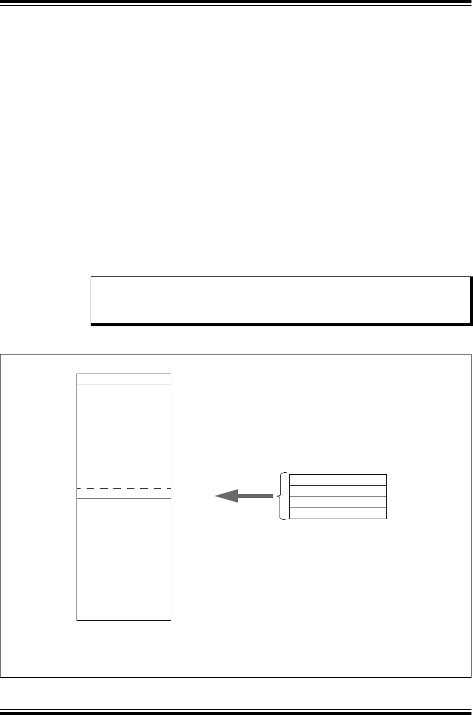
2.3 Flash Configuration Data (PIC24FJ Devices Only)
All PIC24F devices with J-Flash program memory reserve the area at the end of the implemented
program memory range (typically, the last row) for device configuration data. These memory
locations are referred to as Flash Configuration Words. On device Reset, the configuration
information stored in this area is written into the appropriate device Configuration registers, which
are located starting at F80000h in the configuration memory space. In most cases, device
configuration data can only be programmed by programming the desired values to the Flash
Configuration Words.
The number, order and organization of the Flash Configuration Words varies between device
families. Figure 2-3 shows a typical example for Flash Configuration Words with four
implemented words. Refer to the device data sheet for family-specific information.
Figure 2-3: Flash Configuration Words
Note: PIC24F devices with K-Flash memory do not use Flash Configuration Words. The
device Configuration bits are programmed directly at their locations in configuration
memory space (starting at F80000h), using special Table Write instructions or
programming operations. Refer to the specific device data sheet for more details.
000000h
000x00h
Legend: Memory areas are not shown to scale.
Note 1: Exact boundary addresses are determined by the size of the implemented program memory.
Vector Area
7FFFFFh
Flash Configuration Words
xxxx00h
(1)
xxxxFEh
(1)
Unimplemented
Read ‘
0
’
CW1 xxxxx8
CW2 xxxxxA
CW3 xxxxxC
CW4 xxxxxE
User Flash
Program Memory

© 2007-2017 Microchip Technology Inc. DS30009715D-page 7
PIC24F Flash Program Memory
2.4 Memory Organization
The program memory space is organized as word-addressable blocks. Although it is treated as
24 bits wide, it is more appropriate to think of each address of the program memory as a lower
and upper word, with the upper byte of the upper word being unimplemented. The lower word
always has an even address, while the upper word has an odd address (Figure 2-4).
Program memory addresses and the PC are always word-aligned on the lower word (i.e., the LSb
is always ‘0’). Addresses are incremented or decremented by two during code execution.
Figure 2-4: Program Memory Organization
2.4.1 ADDRESSING PROGRAM MEMORY
For normal code execution, the Effective Address (EA) for execution is provided by the Program
Counter (PC). The PC is 23 bits wide, allowing direct access to any location in the user program
space. PC<0> is fixed as ‘0’ in order to maintain program instruction alignment. The PC is
incremented to the next sequential address by incrementing PC<1>, thus increasing the value of
the PC by two.
For Table Read and Table Write operations, the EA is created by concatenating the 16-bit
address from one of the W registers with the 8-bit address from the TBLPAG register. This
permits table operations access to both the user and configuration spaces. Address generation
for table operations is discussed in more detail in Section 3.1 “Address Generation for Table
Operations”.
For Extended Data Space (EDS) and Program Space Visibility (PSV) operations, the EA is
created by concatenating the lower 15 bits of a W register with the 8-bit address from either the
PSVPAG, DSRPAG or DSWPAG registers. Extended Data Space and Program Space Visibility
operations are discussed in the “dsPIC33/PIC24 Family Reference Manual”, “Data Memory
with Extended Data Space (EDS)” (DS39733).
0816
PC Address
000000h
000002h
000004h
000006h
23
00000000
00000000
00000000
00000000
Program Memory
‘Phantom’ Byte
(read as ‘0’)
least significant wordmost significant word
Instruction Width
000001h
000003h
000005h
000007h
msw
Address (lsw Address)
PC Address
(lsw Address)

dsPIC33/PIC24 Family Reference Manual
DS30009715D-page 8 © 2007-2017 Microchip Technology Inc.
3.0 TABLE OPERATION INSTRUCTIONS
The table instructions provide one method of transferring data between the program memory
space and the data memory space of the PIC24F devices. A summary of the table instructions
used during programming of the Flash program memory is provided in this section. There are
four basic table instructions:
• TBLRDL: Table Read Low
• TBLRDH: Table Read High
• TBLWTL: Table Write Low
• TBLWTH: Table Write High
The TBLRDL and the TBLWTL instructions are used to read and write to bits<15:0> of program
memory space. TBLRDL and TBLWTL can access program memory in Word or Byte mode.
The TBLRDH and TBLWTH instructions are used to read or write to bits<23:16> of program memory
space. TBLRDH and TBLWTH can access program memory in Word or Byte mode. Since the
program memory is only 24 bits wide, the TBLRDH and TBLWTH instructions have the ability to
address an upper byte of program memory that does not exist. This byte is called the ‘phantom byte’.
Any read of the phantom byte returns 00h; a write to the phantom byte has no effect.
When any of the table instructions are used in Byte mode, the LSb of the table address will be
used as the byte select bit. The LSb determines which byte in the high or low program memory
space is accessed.
3.1 Address Generation for Table Operations
Figure 3-1 illustrates how the program memory is addressed using the table instructions. A 24-bit
program memory address is formed using the TBLPAG<7:0> bits and the Effective Address (EA)
from a W register, specified in the table instruction (the 24-bit Program Counter is shown for
reference). The upper 23 bits of the EA are used to select the program memory location. For the
Byte mode table instructions, the LSb of the W register EA is used to pick which byte of the 16-bit
program memory word is addressed; ‘1’ selects bits<15:8>, ‘0’ selects bits<7:0>. The LSb of the
W register EA is ignored for a table instruction in Word mode.
In addition to the program memory address, the table instructions also specify a W register (or a
W Pointer to a memory location) that is the source of the program memory data to be written or
the destination for a program memory read. For a Table Write operation in Byte mode, bits<15:8>
of the source Working register are ignored.
Figure 3-1: Addressing for Table Registers
0
Program Counter
24 Bits
Program
TBLPAG Reg
8 Bits
Working Reg EA
16 Bits
Using
Byte
24-Bit EA
0
1/0
Select
Table
Instruction
Counter
Using
User/Configuration
Space Select

© 2007-2017 Microchip Technology Inc. DS30009715D-page 9
PIC24F Flash Program Memory
3.2 Low Word Access
The TBLRDL and TBLWTL instructions are used to access the lower 16 bits of program memory
data. The LSb of the W register address is ignored for word-wide table accesses. For byte-wide
accesses, the LSb of the W register address determines which byte is read. Figure 3-2 illustrates
the program memory data regions accessed by the TBLRDL and TBLWTL instructions.
Figure 3-2: Program Data Table Access (Low Word)
3.3 High Word Access
The TBLRDH and TBLWTH instructions are used to access the upper 8 bits of the program
memory data. These instructions also support Word or Byte Access modes for orthogonality, but
the high byte of the program memory data will always return ‘0’, as shown in Figure 3-3.
Figure 3-3: Program Data Table Access (High Word)
3.4 Table Writes and Write Latches
Table Write instructions do not write directly to the nonvolatile program memory. Instead, the
instructions load holding latches that store the write data. When all of the holding latches have
been loaded, the actual memory programming operation is started by executing a special
sequence of instructions.
The number of write latches implemented determines the type of programming options that are
available (e.g., word, double-word or row) and is device-specific. Refer to the specific device data
sheet for more information.
Holding latches may be implemented in one of two ways: unmapped and memory-mapped. For
unmapped devices, the latches are built into the Flash controller and are not directly addressable;
they can only be accessed using Table Write instructions. The target address for programming is
specified in the programming sequence.
For memory-mapped devices, programming data is written to one or more latches, mapped to a
region in configuration space, starting at FA0000h. The target address for programming is
specified by a special address register.
Specific algorithms for Table Write operations in both unmapped and memory-mapped devices
are covered in subsequent sections.
0816
PC Address
000100h
000102h
000104h
000106h
23
00000000
00000000
00000000
00000000
‘Phantom’ Byte
(Read as ‘0’)
TBLRDL.W
TBLRDL.B (Wn<0> = 1)
TBLRDL.B (Wn<0> = 0)
0816
PC Address
000100h
000102h
000104h
000106h
23
00000000
00000000
00000000
00000000
‘Phantom’ Byte
(Read as ‘0’)
TBLRDH.W
TBLRDH.B (Wn<0> = 1)
TBLRDH.B (Wn<0> = 0)

dsPIC33/PIC24 Family Reference Manual
DS30009715D-page 10 © 2007-2017 Microchip Technology Inc.
3.5 Data Storage in Program Memory
It is assumed that for most applications, the high byte (P<23:16>) will not be used for data,
making the program memory appear 16 bits wide for data storage. It is recommended that the
upper byte of program data be programmed either as a NOP (00h or FFh), or as an illegal opcode
(3Fh) value, to protect the device from accidental execution of stored data. The TBLRDH and
TBLWTH instructions are primarily provided for array program/verification purposes and for those
applications that require compressed data storage.
3.6 Program Memory Bit Behavior
Bits in Flash program memory can only be programmed from ‘1’ to ‘0’ and can be subsequently
erased to ‘1’. Using a programming sequence to set a bit to a ‘1’ will have no effect.
3.7 Using Table Read Instructions
Table Reads require two steps. First, an Address Pointer is set up using the TBLPAG register
and one of the W registers. Then, the program memory contents at the address location may be
read.
The code examples in Example 3-1 and Example 3-2 demonstrate how to read a word of
program memory using the table instructions. These examples use the tblpage() and
tbloffset() directives, which are provided by the Microchip assembler for PIC24F devices.
These directives select the appropriate TBLPAG and W register values for the table instruction
from a program memory address value. Refer to the “MPLAB
®
Assembler, Linker and Utilities for
PIC24 MCUs and dsPIC
®
DSCs User’s Guide” (DS51317) for more information.
Example 3-1: Byte Read (in Assembly)
Example 3-2: Word Read of Variable from Program Memory (in Assembly)
; Read program memory address 0x012340
; Create 24 bit EA for read by loading TBLPAG and W1
MOV #0x0001, W0 ; Load TBLPAG register with read address <23:16>
MOV W0, TBLPAG
MOV #0x2340, W1 ; Load W1 with read address <15:0>
; Read data from program memory into W registers
TBLRDL.B [W1++], W2 ; W2 contains low byte
TBLRDL.B [W1--], W3 ; W3 contains middle byte
TBLRDH.B [W1], W4 ; W4 contains high byte
PROG_DATA: .word 0x1234 ; 16 bit variable in program memory
; Create EA for read by loading TBLPAG and W0
MOV #tblpage(PROG_DATA), W0 ; Get upper byte address of variable PRG_DATA
MOV W0, TBLPAG ; Load upper address into TBLPAG register
MOV #tbloffset(PROG_DATA), W1 ; Load W1 with lower address word
; of variable PRG_DATA
; Read data from program memory
; into W registers
TBLRDL [W1], W2 ; W2 contains 16 bit variable data

© 2007-2017 Microchip Technology Inc. DS30009715D-page 11
PIC24F Flash Program Memory
The code examples in Example 3-3 and Example 3-4 demonstrate how to read a word of
program memory in C. These examples use the MPLAB XC16 C compiler’s
__builtin_tblpage() and __builtin_tbloffset() functions to return the values of
TBLPAG and the offset, and __builtin_tblrdl and __builtin_tblrdh instructions to
access the Table Read assembler instructions. Refer to the “MPLAB
®
XC16 C Compiler User’s
Guide” (DS50002071) for more information.
Example 3-3: Word Read (in C)
Example 3-4: Read of Variable from Program Memory (in C)
3.8 Using Table Write Instructions
Table Write operations differ between devices with unmapped and memory-mapped write latches
in the way that the destination address for programming is specified. In unmapped devices, the
programming target is specified by the TBLPAG and Wn registers. In memory-mapped devices,
the NVMADR/NVMADRU registers specify the target address; TBLPAG and Wn specify the
address of the write latches.
3.8.1 TABLE WRITES WITH UNMAPPED WRITE LATCHES
For unmapped devices, Table Write operations are done in three steps:
1. Load TBLPAG and a Wn register with the 24-bit destination address.
2. Load the Wn register with data or a pointer to write data.
3. Perform the TBLWT instructions to load the write latches.
For word programming, this sequence only needs to be done once, as shown in Example 3-5.
Example 3-5: Loading Write Latches, Word Programming (in Assembly)
int addrOffset, readDataL, readDataH;
// Read 24 bits of data memory from address 0x012340
// Create 24 bit EA for read by loading TBLPAG
TBLPAG = 0x0001; // Load TBLPAG register with read address <23:16>
addrOffset = 0x2340; // Load offset with read address <15:0>
// Read data from program memory
readDataL = __builtin_tblrdl(addrOffset); // readDataL contains lower word data
readDataH = __builtin_tblrdh(addrOffset); // readDataH contains high byte data
int addrOffset, readDataL;
// Create variable in program space at address 0x012340
__prog__int__attribute__ ((space(prog), address(0x012340))) PROG_ADDR = 0xABCD;
// Create 24 bit EA for read by loading TBLPAG
TBLPAG = __builtin_tblpage(&PROG_ADDR); // Load upper address into TBLPAG register
addrOffset = __builtin_tbloffset(&PROG_ADDR); // Mask for word alignment
// Read data from program memory
readDataL = __builtin_tblrdl(addrOffset); // readDataL contains 16 bit variable data
; Set up a pointer to the location to be written (x012340 for this example)
MOV #0x0001, W0
MOV W0, TBLPAG ; Load TBLPAG with upper address
MOV #0x2340, W1 ; Load W1 with lower address word
; Load write data into Wn registers
MOV #WRITE_DATA_1L, W2
MOV #WRITE_DATA_1H, W3
; Perform the TBLWT instructions to load the write latches
TBLWTL W2, [W1]
TBLWTH W3, [W1]

dsPIC33/PIC24 Family Reference Manual
DS30009715D-page 12 © 2007-2017 Microchip Technology Inc.
For devices that support row programming, the sequence is repeated in a loop until all write
latches are written. Example 3-6 loads 64 write latches and uses W1 as a pointer to the write
data. W1 is post-incremented to point to the next byte to be written to the write latch.
Example 3-6: Loading Write Latches, Row Programming (in Assembly)
3.8.2 TABLE WRITES WITH MEMORY-MAPPED LATCHES
Table Write operations are done in three steps:
1. Load TBLPAG and a Wn register with the 24-bit address of the write latch.
2. Load the Wn register with data or a pointer to write data.
3. Perform the TBLWT instructions to load the write latches.
The sequence for double-word programming in Example 3-7 performs Step 3 (TBLWT sequence)
twice to write the second word. For devices that support row programming, the sequence is
repeated in a loop until all write latches are written. Example 3-8 loads 64 write latches and uses
W1 as a pointer to the write data. W1 is post-incremented to point to the next write latch.
Example 3-7: Loading Write Latches, Double-Word Programming (in Assembly)
Example 3-8: Loading Write Latches, Row Programming (in Assembly)
; Set up a pointer to the location to be written (x010200 for this example)
MOV #0x0001, W0
MOV W0, TBLPAG ; Load TBLPAG with upper address
MOV #0x0200, W1 ; Load W1 with lower address word
; Set up write data address pointer, W2 point to data in RAM
MOV #WRITE_ADDR, W2
; Perform the TBLWT instructions to load the write latches
MOV #64, W3 ; Set loop count to number of write latches
loop:
TBLWTL.b [W2++], [W1++] ; Load lower byte to write latch
TBLWTL.b [W2++], [W1--] ; Load middle byte to write latch
TBLWTH.b [W2++], [W1] ; Load high byte to write latch
INC2 W1, W1 ; Increment to next write latch
DEC W3, W3 ; Decrement loop count
BRA NZ, loop
; Set up the address pointer to 1st write latch
MOV 0xFA, W0
MOV W0, TBLPAG ; Load TBLPAG with write latch upper address
MOV 0x0, W0 ; Load W0 with lower write latch address
; Load write data into Wn registers
MOV #PROG_LOW_WORD_1, W2
MOV #PROG_HI_BYTE_1, W3
MOV #PROG_LOW_WORD_2, W4
MOV #PROG_HI_BYTE_2, W5
; Perform the table writes to load the latch
TBLWTL W2, [W0]
TBLWTH W3, [W0++]
TBLWTL W4, [W0]
TBLWTH W5, [W0++]
; Set up a pointer to write latch
MOV #0x00FA, W0
MOV W0, TBLPAG ; Load TBLPAG with upper write latch address
MOV #0x0000, W1 ; Load W1 with lower address word
; Set up write data address pointer, W2 point to data in RAM
MOV #WRITE_ADDR, W2
; Perform the TBLWT instructions to load the write latches
MOV #64, W3 ; Set loop count to number of write latches
loop:
TBLWTL.b [W2++], [W1++] ; Load lower byte to write latch
TBLWTL.b [W2++], [W1--] ; Load middle byte to write latch
TBLWTH.b [W2++], [W1] ; Load high byte to write latch
INC2 W1, W1 ; Increment to next write latch
DEC W3, W3 ; Decrement loop count
BRA NZ, loop

© 2007-2017 Microchip Technology Inc. DS30009715D-page 13
PIC24F Flash Program Memory
4.0 FLASH MEMORY PROGRAMMING
PIC24F devices can be programmed by any one of three methods:
• Run-Time Self-Programming (RTSP)
• In-Circuit Serial Programming™ (ICSP™)
• Enhanced In-Circuit Serial Programming (EICSP)
RTSP is performed by the application software during execution, while ICSP and EICSP are
performed from an external programmer using a serial data connection to the device. ICSP and
EICSP allow much faster programming time than RTSP.
RTSP techniques are described in this section. The ICSP and EICSP protocols are defined in the
Programming Specification documents for the respective devices, which can to be downloaded
from the Microchip web site (www.microchip.com).
4.1 Registers
All programming operations are controlled through two registers: NVMCON and NVMKEY.
4.1.1 NVMCON REGISTER
The NVMCON register (Register 4-1) controls all Flash programming operations. The
NVMOP<5:0> bits field selects the particular write or erase operation to be performed, while the
ERASE bit (NVMCOM<6>) determines if the operation is an erase or program operation.
The WR bit (NVMCOM<15>) triggers the appropriate operation; it remains set until the operation
has been completed and is then cleared by hardware. The WREN bit (NVMCOM<14>) enables
or disables write and erase operations; WR cannot be set to trigger operations when WREN is
clear.
4.1.2 NVMKEY REGISTER
NVMKEY is a write-only register that is used to prevent accidental writes or erasures of Flash
memory; only the lower byte is implemented. To start a program or erase sequence, an “unlock”
sequence of two writes is performed on the register:
1. Write 55h to NVMKEY<7:0>.
2. Write AAh to NVMKEY<7:0>.
After this sequence, a write will be allowed to the NVMCON register for one instruction cycle. The
critical timing of the instruction sequence requires that applications written in C use in-line
assembler directives to directly execute the sequence. Alternatively, the MPLAB XC16
C Compiler includes the built-in function, __builtin_write_NVM, to correctly execute the
sequence, including the setting of the WR bit. For more information, refer to the “MPLAB
®
XC16
C Compiler User’s Guide” (DS50002071).
When initiating a programming or erase operation, it is recommended to first disable all device
interrupts for at least five instruction cycles; this prevents an unexpected hardware event from
interrupting the unlock sequence or setting the WR bit. In assembler, this is accomplished with the
instruction, disi #5. In MPLAB XC16 C Compiler, the built-in function, __builtin_disi(5),
serves the same purpose.
4.1.3 NVMADR AND NVMADRU
For devices with memory-mapped write latches, the NVMADR and NVMADRU registers are
implemented to contain the destination address of a Flash memory write. NVMADR is
implemented as a 16-bit register and contains the lower 16 bits of the 24-bit address. NVMADRU
is also 16 bits, but only implements the lower byte; it contains the upper 8 bits of the address.

dsPIC33/PIC24 Family Reference Manual
DS30009715D-page 14 © 2007-2017 Microchip Technology Inc.
Register 4-1: NVMCON: NVM Flash Programming Control Register
R/S-0
(1)
R/W-0 R/W-0 R/W-0 U-0 U-0 U-0 U-0
WR WREN WRERR
PGMONLY
(2)
— — — —
bit 15 bit 8
U-0 R/W-0 R/W-0 R/W-0 R/W-0 R/W-0 R/W-0 R/W-0
— ERASE NVMOP5
(2)
NVMOP4
(2)
NVMOP3 NVMOP2 NVMOP1 NVMOP0
bit 7 bit 0
Legend: S = Settable Only bit
R = Readable bit W = Writable bit U = Unimplemented bit, read as ‘0’
-n = Value at POR ‘1’ = Bit is set ‘0’ = Bit is cleared x = Bit is unknown
bit 15 WR: Write Control bit
(1)
1 = Initiates a Flash program/erase operation; cleared by hardware upon completion of operation
0 = Program/erase operation is complete and inactive
bit 14 WREN: Program/Erase Enable bit
1 = Allows program/erase cycles
0 = Inhibits programming/erasing of memory or fuse elements
bit 13 WRERR: Sequence Error Flag bit
1 = An improper program/erase termination has occurred or an unimplemented programming operation
has been selected
0 = A program or erase operation is under way, has completed normally or has yet to start
bit 12 PGMONLY: NVM Power-Down in Idle Enable bit
(2)
Not used in Flash program memory operations; available only in devices with data EEPROM.
bit 11-7 Unimplemented: Read as ‘0’
bit 6 ERASE: Erase/Program Enable bit
1 = Performs the erase operation specified by the NVMOPx bits field on the next WR command
0 = Performs the program operation specified by the NVMOPx bits field on the next WR command
bit 5-0 NVMOP<5:0>: NVM Operation Select bits (initiated by the next setting of WR)
(2)
Valid program/erase operations are device-specific. Refer to the specific device data sheet.
Note 1: This bit is also reset on a BOR.
2: The PGMONLY and NVMOP<5:4> bits are not implemented for all versions of Flash memory. Refer to the
specific device data sheet for more information.

© 2007-2017 Microchip Technology Inc. DS30009715D-page 15
PIC24F Flash Program Memory
4.2 Run-Time Self-Programming (RTSP)
RTSP allows the user code to modify Flash program memory contents. RTSP is accomplished
using TBLRD (Table Read) and TBLWT (Table Write) instructions, and the NVM Control registers.
PIC24F devices support the following Flash programming operations:
• Flash Page Erases
• Row Programming (either latch-based or RAM-based)
• Word Programming
• Double-Word Programming (select devices only)
Flash programming via RTSP is performed either with blocks of memory called rows, or with one
or two words of Flash memory. Prior to programming, a memory location must be erased. Erase
operations are performed on blocks of memory called pages, which consist of multiple rows. The
size of a row will vary by device; refer to the device data sheet for details. Typically, for PIC24F
devices, a page is defined as eight (8) rows. This document uses examples with 64 instructions
per row (512 instructions per page).
4.2.1 FLASH PROGRAMMING ALGORITHM AND EXAMPLES
Flash programming operations are controlled using the NVMCON and NVMKEY registers. A
complete programming sequence is necessary for programming or erasing the internal Flash in
RTSP mode. Setting the WR bit (NVMCON<15>) starts the operation and the WR bit is
automatically cleared when the operation is finished.
An erase operation must be performed before Flash writes. Since the smallest erase operation
size is one page, it is necessary for word and row programming operations to temporarily move
the remainder of the page data to RAM, and then write it back to memory. Table Read instructions
can be used to fill a data buffer that can then be written back to memory.
The CPU stalls until the programming operation is finished. The CPU will not execute any
instructions or respond to interrupts during this time. Interrupts that occur during the
programming cycle will remain pending until the cycle completes.
If a POR or BOR event occurs while an RTSP erase or programming operation is in progress,
the RTSP operation is aborted immediately. The user should execute the RTSP operation again
after the device comes out of Reset. If an EXTR, SWR, WDTO, TRAPR, CM or IOPUWR Reset
event occurs while an RTSP erase or programming operation is in progress, the device will be
reset only after the RTSP operation is complete. Two NOP instructions should always follow erase
and program operations.
Programming a page of Flash program memory with RTSP involves three steps:
1. Create a RAM image of the page data to be modified.
2. Erase the page.
3. Program the page.
It is also recommended to verify the data written to memory against the RAM image to ensure
integrity.
Note: On PIC24F devices with J-Flash program memory, erasing the last page of program
memory also erases the Flash Configuration Words. If the device also implements
security features, such as write protection, erasing the Configuration Words may
enable security and prevent further programming changes. Refer to the specific
device data sheet and programming specification for more information on code
security features.

dsPIC33/PIC24 Family Reference Manual
DS30009715D-page 16 © 2007-2017 Microchip Technology Inc.
4.2.2 CREATE A RAM IMAGE
The RAM image must be read starting from a page address boundary. Perform these two steps
to create a RAM image of the data page to be modified:
1. Read the content of the Flash program memory page using Table Read instructions and
store it into data RAM as a data image.
2. Modify the RAM image as required.
4.2.3 ERASE THE PAGE
Page erase operations erase one page (8 rows) of program memory. A page erase should
always be done before any programming operation is started. TBLPAG and one of the W
registers are loaded with the starting address of the page to be erased, and a dummy TBLWT is
executed to load this address into the Flash controller. The program memory must be erased at
an even page address boundary. See the “Flash Program Memory” chapter of the specific
device data sheet to determine the size of the Flash page.
To perform a page erase:
1. Set the NVMOPx bits field for a word program operation (refer to the device data sheet for
the proper value).
2. Set the ERASE bit (NVMCON<6>).
3. For devices with non memory-mapped write latches, write the starting address of the page
to be erased into TBLPAG and a W register, and execute a dummy TBLWT command, as
shown in Example 4-1. For devices with memory-mapped write latches, write the starting
address of the page to be erased into NVMADR/NVMADRU, as shown in Example 4-2.
4. Disable interrupts.
5. Write the key sequence to the NVMKEY register (see Section 4.1.2 “NVMKEY Register”).
6. Set the WR bit (NVMCON<15>) to start the erase cycle.
7. Execute two NOP instructions. The WR bit is cleared when the erase cycle is complete.
Example 4-1: Page Erase Example in C (Unmapped Latches)
Example 4-2: Page Erase Example in C (Mapped Latches)
4.2.3.1 Row Erase
Some PIC24F devices support individual row erases, making it unnecessary to erase the entire
Flash page. The process is similar to the page erase procedure. Refer to the “Flash Program
Memory” chapter of the device data sheet or the device programming specification for availability.
int writeAddressL, writeAddressH;
int offset;
// Set ERASE, WREN and configure NVMOP for page erase (see data sheet)
NVMCON = 0x40xx;
// Set target write address
offset = (writeAddressL & 0xFF00); // Mask to page boundary
TBLPAG = writeAddressH;
__builtin_tblwtl(offset, 0); // Dummy TBLWT to load address
__builtin_disi(5); // Disable interrupts for NVM unlock
__builtin_write_NVM(); // Start write cycle
int writeAddressL, writeAddressH;
int offset;
// Set ERASE, WREN and configure NVMOP for page erase (see data sheet)
NVMCON = 0x40xx;
// Set target write address
NVMADR = (writeAddressL & 0xFF00); // Page address to erase
NVMADRH = writeAddressH;
__builtin_disi(5); // Disable interrupts for NVM unlock
__builtin_write_NVM(); // Start write cycle

© 2007-2017 Microchip Technology Inc. DS30009715D-page 17
PIC24F Flash Program Memory
4.2.4 PROGRAM THE PAGE
After the program memory page has been erased, it can be written to from data RAM with the
updated image. Most commonly, this either involves writing one or two instruction words, or an
entire row.
As with table operations, there are different algorithms for devices with unmapped and
memory-mapped write latches.
4.2.4.1 Single-Word Programming
Single-word programming (Example 4-3) programs a single 24-bit Flash memory location. It is
available only in devices with unmapped write latches. The destination address should be
masked with FFFFFEh to ensure an even address.
To perform:
1. Set the NVMOPx bits field for a word program operation (refer to the device data sheet for
the proper value).
2. Write the destination address to the TBLPAG and a W register.
3. Load write latches with the RAM image write data (see
Section 3.8 “Using Table Write
Instructions”
).
4. Disable interrupts.
5. Write the key sequence to the NVMKEY register (see
Section 4.1.2 “NVMKEY Register”
).
6. Set the WR bit (NVMCOM<15>). This will start the program cycle. The WR bit is cleared
when the erase cycle is complete.
Example 4-3: Single-Word Programming in C
int writeAddressL, writeAddressH;
int writeDataL = 0xXXXX;
int writeDataH = 0x00XX;
int offset;
// Set WREN and NVMOP for double word program mode (see data sheet)
NVMCON = 0x40xx;
// Set target write address
offset = (writeAddressL & 0xFFFE); // Mask to even address
TBLPAG = writeAddressH;
__builtin_tblwtl(offset, writeDataL); // Load write latches
__builtin_tblwth(offset, writeDataH);
__builtin_disi(5); // Disable interrupts for NVM unlock
__builtin_write_NVM(); // Start write cycle

dsPIC33/PIC24 Family Reference Manual
DS30009715D-page 18 © 2007-2017 Microchip Technology Inc.
4.2.4.2 Double-Word Programming
Double-word programming (Example 4-4) programs two 24-bit Flash memory locations. It is only
available on devices with memory-mapped write latches.
To perform:
1. Set the NVMOPx bits field for a double-word program operation (refer to the device data
sheet for the proper value).
2. Write the start address of the write latches to the TBLPAG and Wn registers.
3. Write the destination address to the NVMADR/NVMADRU registers.
4. Load write latches with the RAM image write data (see
Section 3.8 “Using Table Write
Instructions”
).
5. Disable interrupts.
6. Write the key sequence to the NVMKEY register (see
Section 4.1.2 “NVMKEY Register”
).
7. Set the WR bit (NVMCOM<15>). This will start the program cycle. The WR bit is cleared
when the erase cycle is complete.
Example 4-4: Double-Word Programming in C
int writeData1L = 0xXXXX;
int writeData1H = 0x00XX;
int writeData2L = 0xXXXX;
int writeData2H = 0x00XX;
int addrOffset;
int WriteAddressL, WriteAddressH;
NVMCON = 0x40xx; // Set WREN and word program mode
TBLPAG = 0xFA; // Write latch upper address
NVMADRL = WriteAddressL; // Set target write address
NVMADRH = WriteAddressH;
__builtin_tblwtl(0,writeData1L); // Load write latches
__builtin_tblwth(0,writeData1H);
__builtin_tblwtl(0x2,writeData2L);
__builtin_tblwth(0x2,writeData2H);
__builtin_disi(5); // Disable interrupts for NVM unlock
__builtin_write_NVM(); // Initiate write

© 2007-2017 Microchip Technology Inc. DS30009715D-page 19
PIC24F Flash Program Memory
4.2.4.3 Row Programming (Unmapped Write Latches)
Row programming is similar to word programming and utilizes a larger number of write latches
to program a whole row at a time. Eight (8) row programming operations are needed to program
one page. The target address must be on a row boundary start address.
Row programming may be implemented on devices with either unmapped or memory-mapped
write latches. Example 4-5 shows the method for devices with unmapped latches.
To program a row of Flash memory:
1. Set the NVMOPx bits field for a word program operation (refer to the device data sheet for
the proper value).
2. Write the start address of the row to be programmed into the TBLPAG and W registers.
3. Load write latches with the RAM image write data (see
Section 3.8 “Using Table Write
Instructions”
).
4. Disable interrupts.
5. Write the key sequence to the NVMKEY register (see
Section 4.1.2 “NVMKEY Register”
).
6. Set the WR bit (NVMCON<15>) to start the program cycle. The WR bit is cleared when
the erase cycle is complete.
Example 4-5: Row Programming in C with Built-in Functions (Unmapped Latches)
Note:
Not all devices support row programming. Refer to the specific device data sheet
for availability.
int writeDataL[64]; // Lower word write data
char writeDataH[64]; // Upper byte write data
int i, offset, writeAddressL, writeAddressH;
// Set WREN and NVMOP bits for row programming (see data sheet)
NVMCON = 0x40xx;
// Set target write address
offset = (writeAddressL & 0xFF80);
// Mask to start of row
TBLPAG = writeAddressH;
for(i=0; i<=63; i++) // Load 64 write latches with data
{
// Increment program address by 2
__builtin_tblwtl((offset + (i * 2)), writeDataL[i]);
__builtin_tblwth((offset + (i * 2)), writeDataH[i]);
}
__builtin_disi(5); // Disable interrupts for NVM unlock
__builtin_write_NVM(); // Start write cycle

dsPIC33/PIC24 Family Reference Manual
DS30009715D-page 20 © 2007-2017 Microchip Technology Inc.
4.2.4.4 Row Programming (Memory-Mapped Write Latches)
The process for row programming in devices with memory-mapped latches is similar to that for
devices with unmapped latches. Example 4-6 shows the procedure.
To program a row of Flash memory:
1. Set the NVMOPx bits field for a word program operation (the value is device-specific; refer
to the data sheet for the proper value).
2. Write the start address of the write latches to the TBLPAG and Wn registers.
3. Write the start address of the row to be programmed into the NVMADR and NVMADRU
registers.
4. Load write latches with the RAM image write data (see
Section 3.8 “Using Table Write
Instructions”
).
5. Disable interrupts.
6. Write the key sequence to the NVMKEY register (see
Section 4.1.2 “NVMKEY Register”
).
7. Set the WR bit (NVMCON<15>) to start the program cycle. The WR bit is cleared when
the erase cycle is complete.
Example 4-6: Row Programming in C with Built-in Functions (Memory-Mapped)
int varWordL[64];
int varWordH[64];
int WriteAddressL, WriteAddressH;
int i;
NVMCON = 0x40xx; // Set WREN and row program mode
TBLPAG = 0xFA;
NVMADRL = WriteAddressH; // set target write address
NVMADRH = WriteAddressL;
for(i=0; i<=63; i++) // load write latches with data
{ // to be written
__builtin_tblwtl((i * 2), varWordL[i]);
__builtin_tblwth((i * 2), varWordH[i]);
}
__builtin_disi(5); // Disable interrupts
__builtin_write_NVM(); // Start write cycle

© 2007-2017 Microchip Technology Inc. DS30009715D-page 21
PIC24F Flash Program Memory
5.0 PROGRAM SPACE VISIBILITY AND EXTENDED DATA SPACE
(PSV AND EDS)
For all PIC24F devices, table instructions (see
Section 3.0 “Table Operation Instructions”
)
can be used to access data within the program memory space. This is useful when data only
needs to be read or written, one byte or word at a time.
It is also possible to map 16K word pages of the program memory space into the upper 32 Kbytes
of the data address space. This allows an effective expansion of the data space beyond its
normal 64-Kbyte addressing limits, as well as transparent access without the use of table
instructions.
All PIC24F devices are able to map any page in the implemented program memory space into
the data space for read-only access. This feature is known as Program Space Visibility (PSV).
Additionally, some devices expand PSV with read/write access to an extended range of virtual
memory pages. This feature is particularly useful for peripherals, such as the Advanced Graphics
Controller, which has high data throughput requirements. This expansion of PSV is known as
Extended Data Space (EDS).
PSV and EDS are implemented as features of the data memory. For a detailed description, refer
to the “dsPIC33/PIC24 Family Reference Manual”,
“PIC24F Data Memory”
(DS30009717) or
“Data Memory with Extended Data Space (EDS)”
(DS39733).
5.1 PSV and Instruction Stalls
For more information about instruction Stalls using PSV, refer to
“CPU”
(DS39703) in the
“dsPIC33/PIC24 Family Reference Manual”.
6.0 ERROR CORRECTING CODE (ECC)
In order to improve program memory performance and durability, select PIC24F devices include
Error Correcting Code (ECC) functionality as an integral part of the Flash memory controller.
ECC can determine the presence of single bit errors in program data, including which bit is in
error, and correct the data without user intervention. When implemented, ECC is automatic and
cannot be disabled.
When data is written to program memory, the controller generates and stores a 7-bit ECC for
every pair of (24-bit) instruction words. ECC data is not memory-mapped and is inaccessible to
the user. When the data is read back, the controller calculates parity on it and compares it to the
previously stored ECC value. If a mismatch occurs, there are two possible outcomes:
• Single bit errors are automatically identified and corrected on read back.
• Double-bit errors will generate an ECC double-bit error trap.
7.0 LOW-POWER OPERATION
Most PIC24F devices include a feature that allows program memory to be powered down when
the device enters Sleep mode, thereby providing incremental reduction to Power-Down Current
(I
PD
). The feature is controlled by the PMSLP bit (RCON<8>); it is also designated in some
devices as the VREGS bit, but with the same functionality.
When PMSLP is clear, bias voltage is removed from program memory, while the device’s on-chip
voltage regulator enters Standby mode. When the bit is set, program memory remains under bias
while the device is in Sleep mode. While leaving PMSLP clear reduces power-down current, it
also increases the wake-up delay from Sleep.

dsPIC33/PIC24 Family Reference Manual
DS30009715D-page 22 © 2007-2017 Microchip Technology Inc.
8.0 REGISTER MAP
A summary of the Special Function Registers (SFRs) associated with the PIC24F Flash Program Memory is provided in Table 8-1 .
Table 8-1: Special Function Registers Associated with Flash Program Memory
(1)
File
Name
Bit 15 Bit 14 Bit 13 Bit 12 Bit 11 Bit 10 Bit 9 Bit 8 Bit 7 Bit 6 Bit 5 Bit 4 Bit 3 Bit 2 Bit 1 Bit 0
All
Resets
(2)
TBLPAG — — — — — — — — Table Page Address Pointer 0000
NVMCON WR WREN WRERR NVMPIDL
PGMONLY
(3)
— — — — ERASE NVMOP5
(3)
NVMOP4
(3)
NVMOP3 NVMOP2 NVMOP1 NVMOP0 0000
NVMKEY
— — — — — — — — NVMKEY<7:0> 0000
NVMADR Flash Program Memory Destination Address Register, Lower Word 0000
NVMADRU
— — — — — — — — Flash Program Memory Destination Address Register, Upper Byte --00
Legend: — = unimplemented, read as ‘0’. Reset values are shown in hexadecimal.
Note 1: Please refer to the device data sheet for specific memory map details.
2: Reset value shown is for POR only. Value on other Reset states is dependent on the state of memory write or erase operations at the time of Reset.
3: Not implemented on all devices; refer to the specific device data sheet for more information.

© 2007-2017 Microchip Technology Inc. DS30009715D-page 23
PIC24F Flash Program Memory
9.0 RELATED APPLICATION NOTES
This section lists application notes that are related to this section of the manual. These
application notes may not be written specifically for the dsPIC33 or PIC24 product families, but
the concepts are pertinent and could be used with modification and possible limitations.
The current application notes related to the PIC24F Flash Program Memory are:
Title Application Note #
No related application notes at this time.
Note:
Please visit the Microchip web site (www.microchip.com) for additional Application
Notes and code examples for the dsPIC33 and PIC24 families of devices.

dsPIC33/PIC24 Family Reference Manual
DS30009715D-page 24 © 2007-2017 Microchip Technology Inc.
10.0 REVISION HISTORY
Revision A (January 2007)
This is the initial released revision of this document.
Revision B (July 2010)
This revision includes the following updates:
• Updated the following sections to include information on devices with only one holding
latch:
- Section 4.6.2.1 “Table Write Holding Latches”
- Section 4.6.2.2 “Writing a Single Program Memory Latch in Word/Byte Mode”
• Updated
Section
4.6.3.1 “RTSP Operation”
to include information on devices with
multiple holding latches
• Notes:
- Added a note with information to customers for utilizing family reference manual
sections and data sheets as a joint reference (see note above
Section 4.1 “Program
Memory Address Map”
).
- Added a shaded note on availability of PSV in devices with EDS after the first
paragraph in
Section 4.4 “Program Space Visibility (PSV) from Data Space”
.
- Added Note 4 to the Nonvolatile Flash Memory Control Register (see Register 4-1).
- Added Note 3 to the shaded note in
Section 4.7.1 “Flash Row Program Memory
Programming Algorithm”
.
• Minor edits to text and formatting have been incorporated throughout the document
Revision C (April 2015)
Complete revision of the document to parallel the updated structure of the Dual Partition program
memory description presented in
“Dual Partition Flash Program Memory”
(DS70005156).
Contents are also updated to include information on PIC24F K-Flash devices.
Updates the title to “PIC24F Flash Program Memory” for clarity.
Updates the document format and removes the previously assigned master section number as
part of the realignment of PIC24 technical documentation. The document reference number
format is also updated.
Major systemic changes to content include:
• The default program memory map in previous revisions has been redesigned (Figure 2-1)
to more closely reflect the presentation shown in device data sheets.
•
Section 2.1 “Vector Area”
has been greatly expanded, and Figure 2-2 added, to cover the
two versions of IVT mapping that now exist in PIC24F devices (subsequent figures are
renumbered accordingly).
• The discussion of Flash Configuration Words for J-Flash devices has been added.
• Discussion of write latches for Table Write operations is moved to
Section 3.4 “Table
Writes and Write Latches”
, and expanded to differentiate between the use of
memory-mapped and unmapped write latches.
•
Section 3.8 “Using Table Write Instructions”
and
Section 4.2 “Run-Time
Self-Programming (RTSP)”
have been extensively updated to include references to
double-word programming, and to differentiate between devices with memory-mapped and
unmapped write latches. Example 3-7, Example 3-8, Example 4-5 and Example 4-6 are
added as part of this update.
• The discussion of Program Space Visibility (PSV) in previous versions has been moved in
its entirety to
“PIC24F Data Memory”
(DS30009717).
• All existing code examples have been updated to reflect changes in Microchip’s
development tools.
• The discussion of operation in Low-Power modes has been added.
Minor typographic corrections and updates are also incorporated throughout the document.


dsPIC33/PIC24 Family Reference Manual
DS30009715D-page 26 © 2007-2017 Microchip Technology Inc.
NOTES:

2007-2017 Microchip Technology Inc. DS30009715D-page 27
Information contained in this publication regarding device
applications and the like is provided only for your convenience
and may be superseded by updates. It is your responsibility to
ensure that your application meets with your specifications.
MICROCHIP MAKES NO REPRESENTATIONS OR
WARRANTIES OF ANY KIND WHETHER EXPRESS OR
IMPLIED, WRITTEN OR ORAL, STATUTORY OR
OTHERWISE, RELATED TO THE INFORMATION,
INCLUDING BUT NOT LIMITED TO ITS CONDITION,
QUALITY, PERFORMANCE, MERCHANTABILITY OR
FITNESS FOR PURPOSE. Microchip disclaims all liability
arising from this information and its use. Use of Microchip
devices in life support and/or safety applications is entirely at
the buyer’s risk, and the buyer agrees to defend, indemnify and
hold harmless Microchip from any and all damages, claims,
suits, or expenses resulting from such use. No licenses are
conveyed, implicitly or otherwise, under any Microchip
intellectual property rights unless otherwise stated.
Trademarks
The Microchip name and logo, the Microchip logo, AnyRate, AVR,
AVR logo, AVR Freaks, BeaconThings, BitCloud, CryptoMemory,
CryptoRF, dsPIC, FlashFlex, flexPWR, Heldo, JukeBlox, K
EE
L
OQ
,
K
EE
L
OQ
logo, Kleer, LANCheck, LINK MD, maXStylus,
maXTouch, MediaLB, megaAVR, MOST, MOST logo, MPLAB,
OptoLyzer, PIC, picoPower, PICSTART, PIC32 logo, Prochip
Designer, QTouch, RightTouch, SAM-BA, SpyNIC, SST, SST
Logo, SuperFlash, tinyAVR, UNI/O, and XMEGA are registered
trademarks of Microchip Technology Incorporated in the U.S.A.
and other countries.
ClockWorks, The Embedded Control Solutions Company,
EtherSynch, Hyper Speed Control, HyperLight Load, IntelliMOS,
mTouch, Precision Edge, and Quiet-Wire are registered
trademarks of Microchip Technology Incorporated in the U.S.A.
Adjacent Key Suppression, AKS, Analog-for-the-Digital Age, Any
Capacitor, AnyIn, AnyOut, BodyCom, chipKIT, chipKIT logo,
CodeGuard, CryptoAuthentication, CryptoCompanion,
CryptoController, dsPICDEM, dsPICDEM.net, Dynamic Average
Matching, DAM, ECAN, EtherGREEN, In-Circuit Serial
Programming, ICSP, Inter-Chip Connectivity, JitterBlocker,
KleerNet, KleerNet logo, Mindi, MiWi, motorBench, MPASM, MPF,
MPLAB Certified logo, MPLIB, MPLINK, MultiTRAK, NetDetach,
Omniscient Code Generation, PICDEM, PICDEM.net, PICkit,
PICtail, PureSilicon, QMatrix, RightTouch logo, REAL ICE, Ripple
Blocker, SAM-ICE, Serial Quad I/O, SMART-I.S., SQI,
SuperSwitcher, SuperSwitcher II, Total Endurance, TSHARC,
USBCheck, VariSense, ViewSpan, WiperLock, Wireless DNA, and
ZENA are trademarks of Microchip Technology Incorporated in the
U.S.A. and other countries.
SQTP is a service mark of Microchip Technology Incorporated in
the U.S.A.
Silicon Storage Technology is a registered trademark of Microchip
Technology Inc. in other countries.
GestIC is a registered trademark of Microchip Technology
Germany II GmbH & Co. KG, a subsidiary of Microchip Technology
Inc., in other countries.
All other trademarks mentioned herein are property of their
respective companies.
© 2007-2017, Microchip Technology Incorporated, All Rights
Reserved.
ISBN: 978-1-5224-2167-2
Note the following details of the code protection feature on Microchip devices:
• Microchip products meet the specification contained in their particular Microchip Data Sheet.
• Microchip believes that its family of products is one of the most secure families of its kind on the market today, when used in the
intended manner and under normal conditions.
• There are dishonest and possibly illegal methods used to breach the code protection feature. All of these methods, to our
knowledge, require using the Microchip products in a manner outside the operating specifications contained in Microchip’s Data
Sheets. Most likely, the person doing so is engaged in theft of intellectual property.
• Microchip is willing to work with the customer who is concerned about the integrity of their code.
• Neither Microchip nor any other semiconductor manufacturer can guarantee the security of their code. Code protection does not
mean that we are guaranteeing the product as “unbreakable.”
Code protection is constantly evolving. We at Microchip are committed to continuously improving the code protection features of our
products. Attempts to break Microchip’s code protection feature may be a violation of the Digital Millennium Copyright Act. If such acts
allow unauthorized access to your software or other copyrighted work, you may have a right to sue for relief under that Act.
Microchip received ISO/TS-16949:2009 certification for its worldwide
headquarters, design and wafer fabrication facilities in Chandler and
Tempe, Arizona; Gresham, Oregon and design centers in California
and India. The Company’s quality system processes and procedures
are for its PIC
®
MCUs and dsPIC
®
DSCs, KEELOQ
®
code hopping
devices, Serial EEPROMs, microperipherals, nonvolatile memory and
analog products. In addition, Microchip’s quality system for the design
and manufacture of development systems is ISO 9001:2000 certified.
QUALITY MANAGEMENT S
YSTEM
CERTIFIED BY DNV
== ISO/TS 16949 ==

DS30009715D-page 28 2007-2017 Microchip Technology Inc.
AMERICAS
Corporate Office
2355 West Chandler Blvd.
Chandler, AZ 85224-6199
Tel: 480-792-7200
Fax: 480-792-7277
Technical Support:
http://www.microchip.com/
support
Web Address:
www.microchip.com
Atlanta
Duluth, GA
Tel: 678-957-9614
Fax: 678-957-1455
Austin, TX
Tel: 512-257-3370
Boston
Westborough, MA
Tel: 774-760-0087
Fax: 774-760-0088
Chicago
Itasca, IL
Tel: 630-285-0071
Fax: 630-285-0075
Dallas
Addison, TX
Tel: 972-818-7423
Fax: 972-818-2924
Detroit
Novi, MI
Tel: 248-848-4000
Houston, TX
Tel: 281-894-5983
Indianapolis
Noblesville, IN
Tel: 317-773-8323
Fax: 317-773-5453
Tel: 317-536-2380
Los Angeles
Mission Viejo, CA
Tel: 949-462-9523
Fax: 949-462-9608
Tel: 951-273-7800
Raleigh, NC
Tel: 919-844-7510
New York, NY
Tel: 631-435-6000
San Jose, CA
Tel: 408-735-9110
Tel: 408-436-4270
Canada - Toronto
Tel: 905-695-1980
Fax: 905-695-2078
ASIA/PACIFIC
Asia Pacific Office
Suites 3707-14, 37th Floor
Tower 6, The Gateway
Harbour City, Kowloon
Hong Kong
Tel: 852-2943-5100
Fax: 852-2401-3431
Australia - Sydney
Tel: 61-2-9868-6733
Fax: 61-2-9868-6755
China - Beijing
Tel: 86-10-8569-7000
Fax: 86-10-8528-2104
China - Chengdu
Tel: 86-28-8665-5511
Fax: 86-28-8665-7889
China - Chongqing
Tel: 86-23-8980-9588
Fax: 86-23-8980-9500
China - Dongguan
Tel: 86-769-8702-9880
China - Guangzhou
Tel: 86-20-8755-8029
China - Hangzhou
Tel: 86-571-8792-8115
Fax: 86-571-8792-8116
China - Hong Kong SAR
Tel: 852-2943-5100
Fax: 852-2401-3431
China - Nanjing
Tel: 86-25-8473-2460
Fax: 86-25-8473-2470
China - Qingdao
Tel: 86-532-8502-7355
Fax: 86-532-8502-7205
China - Shanghai
Tel: 86-21-3326-8000
Fax: 86-21-3326-8021
China - Shenyang
Tel: 86-24-2334-2829
Fax: 86-24-2334-2393
China - Shenzhen
Tel: 86-755-8864-2200
Fax: 86-755-8203-1760
China - Wuhan
Tel: 86-27-5980-5300
Fax: 86-27-5980-5118
China - Xian
Tel: 86-29-8833-7252
Fax: 86-29-8833-7256
ASIA/PACIFIC
China - Xiamen
Tel: 86-592-2388138
Fax: 86-592-2388130
China - Zhuhai
Tel: 86-756-3210040
Fax: 86-756-3210049
India - Bangalore
Tel: 91-80-3090-4444
Fax: 91-80-3090-4123
India - New Delhi
Tel: 91-11-4160-8631
Fax: 91-11-4160-8632
India - Pune
Tel: 91-20-3019-1500
Japan - Osaka
Tel: 81-6-6152-7160
Fax: 81-6-6152-9310
Japan - Tokyo
Tel: 81-3-6880- 3770
Fax: 81-3-6880-3771
Korea - Daegu
Tel: 82-53-744-4301
Fax: 82-53-744-4302
Korea - Seoul
Tel: 82-2-554-7200
Fax: 82-2-558-5932 or
82-2-558-5934
Malaysia - Kuala Lumpur
Tel: 60-3-6201-9857
Fax: 60-3-6201-9859
Malaysia - Penang
Tel: 60-4-227-8870
Fax: 60-4-227-4068
Philippines - Manila
Tel: 63-2-634-9065
Fax: 63-2-634-9069
Singapore
Tel: 65-6334-8870
Fax: 65-6334-8850
Taiwan - Hsin Chu
Tel: 886-3-5778-366
Fax: 886-3-5770-955
Taiwan - Kaohsiung
Tel: 886-7-213-7830
Taiwan - Taipei
Tel: 886-2-2508-8600
Fax: 886-2-2508-0102
Thailand - Bangkok
Tel: 66-2-694-1351
Fax: 66-2-694-1350
EUROPE
Austria - Wels
Tel: 43-7242-2244-39
Fax: 43-7242-2244-393
Denmark - Copenhagen
Tel: 45-4450-2828
Fax: 45-4485-2829
Finland - Espoo
Tel: 358-9-4520-820
France - Paris
Tel: 33-1-69-53-63-20
Fax: 33-1-69-30-90-79
France - Saint Cloud
Tel: 33-1-30-60-70-00
Germany - Garching
Tel: 49-8931-9700
Germany - Haan
Tel: 49-2129-3766400
Germany - Heilbronn
Tel: 49-7131-67-3636
Germany - Karlsruhe
Tel: 49-721-625370
Germany - Munich
Tel: 49-89-627-144-0
Fax: 49-89-627-144-44
Germany - Rosenheim
Tel: 49-8031-354-560
Israel - Ra’anana
Tel: 972-9-744-7705
Italy - Milan
Tel: 39-0331-742611
Fax: 39-0331-466781
Italy - Padova
Tel: 39-049-7625286
Netherlands - Drunen
Tel: 31-416-690399
Fax: 31-416-690340
Norway - Trondheim
Tel: 47-7289-7561
Poland - Warsaw
Tel: 48-22-3325737
Romania - Bucharest
Tel: 40-21-407-87-50
Spain - Madrid
Tel: 34-91-708-08-90
Fax: 34-91-708-08-91
Sweden - Gothenberg
Tel: 46-31-704-60-40
Sweden - Stockholm
Tel: 46-8-5090-4654
UK - Wokingham
Tel: 44-118-921-5800
Fax: 44-118-921-5820
Worldwide Sales and Service
11/07/16
